
The band theory It is the one that defines the electronic structure of the solid as a whole. It can be applied to any type of solid, but it is in metals where its greatest successes are reflected. According to this theory, the metallic bond results from the electrostatic attraction between the positively charged ions, and the mobile electrons in the crystal..
Therefore, the metallic crystal has a "sea of electrons", which can explain its physical properties. The image below illustrates the metallic link. The purple dots of the electrons are delocalized in a sea that surrounds the positively charged metal atoms.
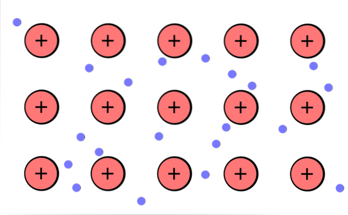
The "sea of electrons" is formed from the individual contributions of each metal atom. These inputs are your atomic orbitals. Metal structures are generally compact; the more compact they are, the greater the interactions between their atoms.
Consequently, their atomic orbitals overlap to generate very narrow molecular orbitals in energy. The sea of electrons is then nothing more than a large set of molecular orbitals with different ranges of energies. The range of these energies make up what is known as energy bands.
These bands are present in any regions of the crystal, which is why it is considered as a whole, and from there comes the definition of this theory.
Article index
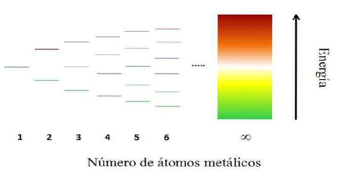
When the s orbital of a metallic atom interacts with that of its neighbor (N = 2), two molecular orbitals are formed: one of bond (green band) and another of anti-bond (dark red band).
If N = 3, three molecular orbitals are now formed, of which the middle one (black band) is non-bonding. If N = 4, four orbitals are formed and the one with the highest binding character and the one with the highest anti-bonding character are further separated..
The range of energy available for molecular orbitals widens as the metal atoms in the crystal contribute their orbitals. This also results in a decrease in the energetic space between the orbitals, to the point that they condense into a band..
This band composed of s orbitals has regions of low energy (those colored green and yellow) and high energy (those colored orange and red). Its energetic extremes have low density; however, most of the molecular orbitals are concentrated in the center (white band).
This means that the electrons “run faster” through the center of the band than through its ends..
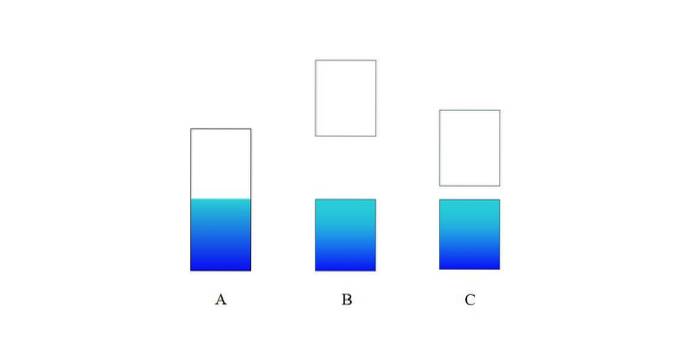
It is the highest energetic state occupied by electrons in a solid at the temperature of absolute zero (T = 0 K).
Once the s band is built, the electrons begin to occupy all of its molecular orbitals. If the metal has a single valence electron (s1), all the electrons in its crystal will occupy half of the band.
The other unoccupied half is known as the conduction band, while the electron-filled band is called the valence band..
In the upper image A represents a typical valence (blue) and conduction (white) band for a metal. The bluish border line indicates the Fermi level.
Since metals also have p orbitals, they combine in the same way to form a p band (white).
In the case of metals, the s and p bands are very close in energy. This allows for their overlaps, promoting electrons from the valence band to the conduction band. This happens even at temperatures just above 0 K.
For transition metals and period 4 downward, d-band formation is also possible.
The Fermi level with respect to the conduction band is of utmost importance in determining the electrical properties.
For example, a metal Z with a Fermi level very close to the conduction band (the closest empty band in energy), has greater electrical conductivity than a metal X in which its Fermi level is far from said band..
Electrical conductivity then consists of the migration of electrons from a valence band to a conduction band.
If the energy gap between the two bands is very large, you have an insulating solid (as with B). On the other hand, if this gap is relatively small, the solid is a semiconductor (in the case of C).
Faced with an increase in temperature, the electrons in the valence band acquire enough energy to migrate towards the conduction band. This results in an electric current.
In fact, this is a quality of solids or semiconductor materials: at room temperature they are insulating, but at high temperatures they are conductive..
Intrinsic conductors are those in which the energy gap between the valence band and the conduction band is small enough for the thermal energy to allow the passage of electrons..
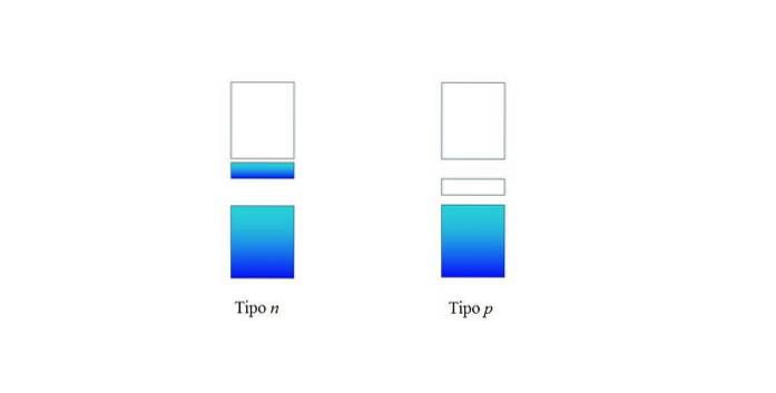
On the other hand, extrinsic conductors exhibit changes in their electronic structures after doping with impurities, which increase their electrical conductivity. This impurity can be another metal or a non-metallic element.
If the impurity has more valence electrons, it can provide a donor band that serves as a bridge for the electrons in the valence band to cross into the conduction band. These solids are n-type semiconductors. Here the denomination n comes from "negative".
In the upper image the donor band is illustrated in the blue block just below the conduction band (Type n).
On the other hand, if the impurity has fewer valence electrons, it provides an acceptor band, which shortens the energy gap between the valence band and the conduction band..
The electrons first migrate towards this band, leaving behind “positive holes”, which move in the opposite direction..
Since these positive holes mark the passage of electrons, the solid or material is a p-type semiconductor.
- Explain why metals are bright: Their moving electrons can absorb radiation over a wide range of wavelengths when they jump to higher energy levels. They then emit light, returning to lower levels of the conduction band.
- Crystalline silicon is the most important semiconductor material. If a portion of silicon is doped with traces of a group 13 element (B, Al, Ga, In, Tl), it becomes a p-type semiconductor. Whereas if it is doped with an element of group 15 (N, P, As, Sb, Bi) it becomes an n-type semiconductor.
- Light-emitting diode (LED) is a p-n board semiconductor. What does it mean? That the material has both types of semiconductors, both n and p. Electrons migrate from the conduction band of the n-type semiconductor to the valence band of the p-type semiconductor.


Yet No Comments